(China (Mainland))


Product Summary
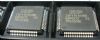
The K7M803625B-QC75 is a 9,437,184 bits Synchronous Static SRAM. The NtRAMTM, or No Turnaround Random Access Memory utilizes all the bandwidth in any combination of operating cycles. Address, data inputs, and all control signals except output enable and linear burst order are synchronized to input clock. Burst order control must be tied High or Low. Asynchronous inputs include the sleep mode enable(ZZ). The K7M803625B-QC75 Output Enable controls the outputs at any given time. Write cycles are internally self-timed and initiated by the rising edge of the clock input. The K7M803625B-QC75 feature eliminates complex offchip write pulse generation and provides increased timing flexibility for incoming signals.
Parametrics
K7M803625B-QC75 absolute maximum ratings: (1)Voltage on VDD Supply Relative to VSS VDD: -0.3 to 4.6 V; (2)Voltage on Any Other Pin Relative to VSS VIN: -0.3 to VDD+0.3 V; (3)Power Dissipation PD: 1.6 W; (4)Storage Temperature TSTG: -65 to 150 °C; (5)Operating Temperature Commercial TOPR: 0 to 70 °C; (6)Operating Temperature Industrial TOPR: -40 to 85 °C; (7)Storage Temperature Range Under Bias TBIAS: -10 to 85 °C.
Features
K7M803625B-QC75 features: (1) 3.3V+0.165V/-0.165V Power Supply; (2) I/O Supply Voltage 3.3V+0.165V/-0.165V for 3.3V I/O or 2.5V+0.4V/-0.125V for 2.5V I/O; (3) Byte Writable Function; (4) Enable clock and suspend operation; (5) Single READ/WRITE control pin.; (6) Self-Timed Write Cycle; (7) Three Chip Enable for simple depth expansion with no data contention; (8) A interleaved burst or a linear burst mode; (9) Asynchronous output enable control; (10) Power Down mode; (11) 100-TQFP-1420A; (12) Operating in commercial and industrial temperature range.
Diagrams

 |
 K7M801825B |
Other |
|
Data Sheet |
Negotiable |
|
||||
|
K7M803625B |
Other |
|
Data Sheet |
Negotiable |
|
||||